Contents
Every phone, car and data centre runs on chips: small slices of silicon carrying billions of microscopic switches called transistors. Making them is one of the most complicated manufacturing processes ever developed. It takes months, hundreds of steps and some of the most complex machines ever built. This article follows a chip from a bare disc of silicon to a finished product.
Starting with a wafer
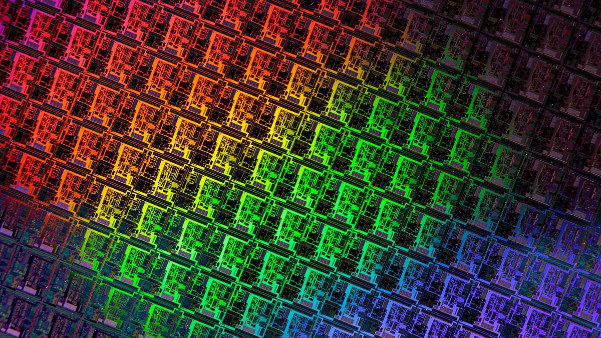
Chips begin as a wafer, a thin, polished disc of extremely pure silicon. According to ASML, the Dutch company that makes the most important machines in the process, the size most often used is 300mm across. Many chips are made on each wafer at once. Depending on how big each chip is, one wafer can hold thousands of them or just a few dozen.
The work happens in factories called fabs, or fabrication plants. The patterns being printed are so small that a speck of dust would ruin them, so fabs are kept extremely clean.
Building up the layers
A chip is not carved out in one go. It is built in layers, one on top of another, and ASML says chips are made up of dozens of them. Each layer goes through the same basic cycle.
- Deposition. A very thin film of material is laid over the wafer. It may conduct electricity, block it, or do something in between.
- Coating. The wafer is covered with a light-sensitive chemical called resist.
- Lithography. Light is shone through a stencil carrying the circuit pattern, called a reticle, and projected onto the resist. Where the light lands, the resist changes.
- Etching. The affected resist is removed, and the exposed material beneath is etched away, leaving the pattern cut into the wafer.
- Ion implantation. Charged particles are fired into the silicon to change its electrical properties in precise places. This is how the transistors themselves are formed.
The cycle is repeated for every layer, with measurement and inspection in between. Finally comes packaging: the wafer is cut into individual chips, each one is mounted on a base that connects it to the outside world, and a cover is fitted to carry heat away.
Those timings come from the Semiconductor Industry Association, the US industry body. They explain why chip shortages cannot be fixed quickly. Even with a factory already running, it takes months for an extra order to come out of the other end.
Lithography: printing with light
Lithography is the step that decides how small the transistors can be, and it is where the most advanced technology sits. The finer the pattern, the shorter the wavelength of light needed to print it, in the way that a fine pen draws thinner lines than a thick one.
ASML sets out the light sources used:
| Type | Wavelength |
|---|---|
| Deep ultraviolet (krypton fluoride laser) | 248 nanometres |
| Deep ultraviolet (argon fluoride laser) | 193 nanometres |
| Extreme ultraviolet (EUV) | 13.5 nanometres |
A nanometre is a millionth of a millimetre. EUV light has a wavelength more than fourteen times shorter than the deep ultraviolet light before it, which is what allows today’s most advanced chips to be made.
Producing EUV light is extraordinarily hard. Inside the machine, molten droplets of tin about 25 microns, or 0.025 millimetres, across fall at around 70 metres a second. A laser pulse flattens each droplet, and a second, stronger pulse turns it into a plasma that gives off EUV light. This happens 50,000 times a second. ASML describes EUV as a technology entirely unique to the company, which makes it the only supplier of the machines every leading-edge chipmaker needs.
Molten droplets of tin are hit by a laser 50,000 times a second to make the light that prints the most advanced chips.”
| Item | Nanometres |
|---|---|
| Deep ultraviolet, krypton fluoride | 248 nm |
| Deep ultraviolet, argon fluoride | 193 nm |
| Extreme ultraviolet | 13.5 nm |
Shorter light prints finer patterns.Source: ASML. Chart: The Sidelight.
What “3 nanometre” really means
Chipmakers label each new generation of manufacturing with a number, such as 7, 5 or 3 nanometres, known as the node. It is natural to assume this is the size of something on the chip. It is not.
IEEE Spectrum, the magazine of the engineering body IEEE, explains that node numbers once matched real dimensions of the transistor, but the two began to come apart in the mid-1990s. Most of the critical features of a so-called 7-nanometre transistor are considerably larger than 7 nanometres. The numbers continued to shrink on their old schedule, but they became a label for a generation, not a measurement. A smaller number still means a more advanced process, but the names of different companies’ processes are not directly comparable.
Why so few companies can do it
Making leading-edge chips needs enormous sums of money, rare expertise and equipment that only a handful of suppliers make. The scale of investment is clear from TSMC, the Taiwanese company that makes chips for other firms. In March 2025 it announced plans to raise its investment in the United States to $165 billion, covering new fabs, two advanced packaging plants and a research centre.
Each generation is harder and dearer than the last, and the yield, the share of chips on a wafer that work, has to be high for a factory to make money. A company that falls behind for a generation or two finds it very hard to catch up. That is why the most advanced chips are made by so few firms in so few places, which is the subject of a companion article on who makes the world’s chips.
The short version
- A chip is built in layers on a silicon wafer, by repeating a cycle of depositing, coating, printing with light, etching and implanting.
- Lithography, printing the pattern with light, sets the limit on how small transistors can be.
- The most advanced chips are printed with extreme ultraviolet light, from machines made only by ASML.
- The whole process can take up to six months from order to delivery, which is why supply cannot respond quickly.
References and sources
- 016 crucial steps in semiconductor manufacturing · ASML · Updated 4 October 2023
- 02Light and lasers · ASML · Accessed 13 November 2026
- 03Chipmakers Are Ramping Up Production to Address Semiconductor Shortage. Here’s Why that Takes Time · Semiconductor Industry Association · 26 February 2021
- 04A Better Way to Measure Progress in Semiconductors · IEEE Spectrum · 21 July 2020
- 05TSMC Intends to Expand Its Investment in the United States to US$165 Billion to Power the Future of AI · TSMC · 4 March 2025
- 06Lead image: 5C2A5953R - 49913961083 – Silicon Wafer 20200519.jpg · Rob Bulmahn, via Wikimedia Commons (CC BY 2.0) · Accessed 13 November 2026
House byline
Articles under this byline are researched and drafted with AI assistance, with every figure checked against its source before publication. The editor, Pankaj Guleria, reviews them and corrects them where needed.
Edited by Pankaj Guleria, Founder and Editor